ASML and TSMC want to expand the "negative" that is used to manufacture d
ASML and TSMC prepare large photomasks to speed up the production of the future daia chips. Here is the innovation, its timeline and its limitations.
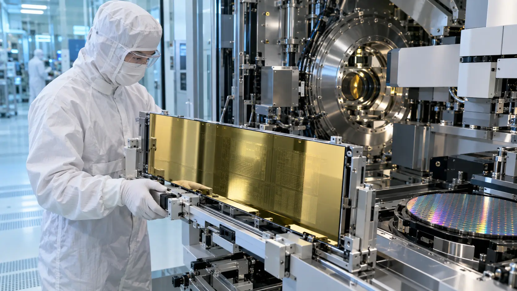
To make a processor, a lithography machine projects patterns on silicon from a plate called photomasque. It can be compared with a photographic negative of extreme accuracy.
ASML and TSMC announced on September 8, 2026 an initiative to move this mask from a standard 6-inch format to an extended 6 × 12-inch format.
The aim is to enable high-NA UV machines to produce very large chips for data centres and artificial intelligence more efficiently.
However, this technology will not be ready tomorrow: a pilot line is targeted for 2031 and advanced production for 2033.
Why do you need a photomask?
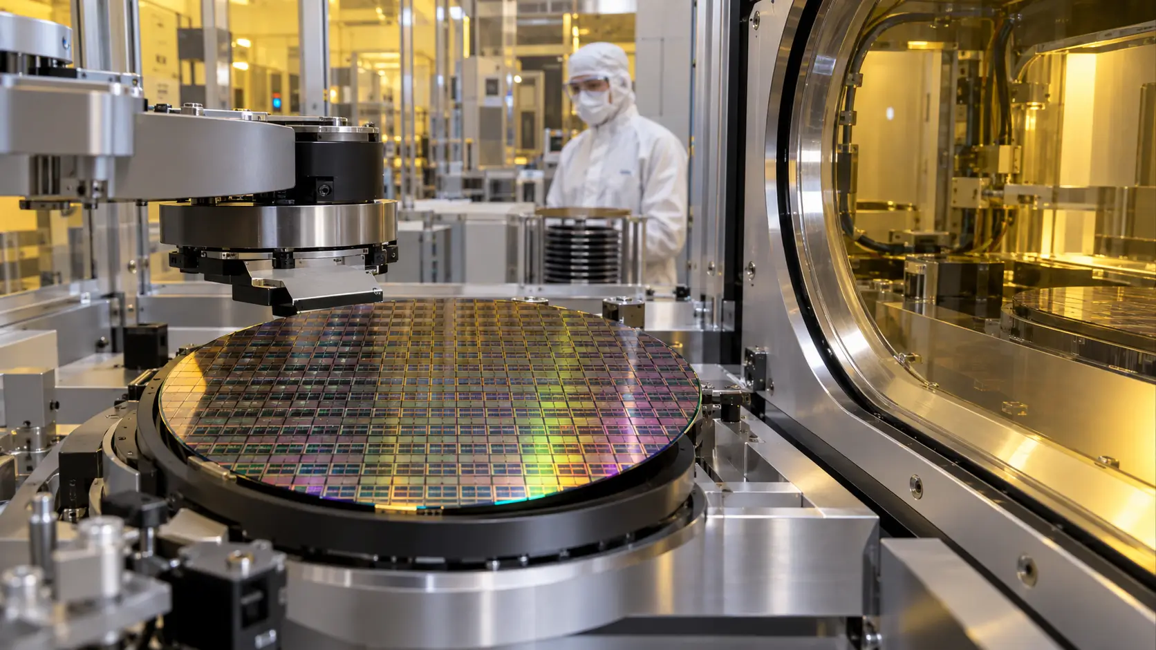
A modern processor brings together billions of transistors. To produce them, successive layers of circuits must be printed on a silicon plate with a precision of a few nanometers.
The UV machines of the ASML use an extreme ultraviolet light with a wavelength of 13.5 nanometers. Since this light is absorbed by almost all materials, the mask does not function as a transparent slide: it reflects light by means of layers of extremely thin materials.
Each mask contains the pattern of a manufacturing step. An advanced chip may require many masks and dozens of exposures before it is finished.
High-NA produces finer details
The new High-NA UV machines increase the digital opening of their optical system from 0.33 to 0.55. This value measures the ability of mirrors to collect and concentrate light.
According to the technical explanation of ASML, this platform can print 8 nanometre details. The manufacturer states that it will allow 1.7 times smaller structures and a theoretical density of transistors 2.9 times higher than that of its previous UV generation.
These comparisons are from ASML. The efficiency of a commercial chip also depends on its design, materials, number of layers, defect rate and the process used by the foundry.
Intel already uses High-NA on some layers of Core Ultra processors manufactured with its 18A process. The company claims to have treated more than one million platelets, but this total includes machine certification, research, development and part of production.
The problem of half-field
To keep the current 6-inch masks, ASML has designed an anamorphic optical system. The image is reduced four times in one direction and eight times in the other.
This solution achieves the desired accuracy, but cuts the printable surface in half during a single exposure.
A little chip can enter this half-field. Rather, a large chip from the AI must be divided into two patterns, then assembled on silicon by a technique called "stitching", or lithographic assembly.
This junction requires extremely precise alignment. It complicates design, increases exposures and can reduce productivity.
Current UV machines can produce chips around 800 mm2. NVIDIA, Google and other designers already use almost this entire area for some data centre accelerators, according to [Reuters] (https://www.reuters.com/world/asia-pacific/asml-work-with-major-chipmakers-to-use-latest-tools-larger-chips-2026-09-08/).
#A mask twice as long
The 6 × 12 inches format should give the High-NA machines a full field for large chips.
ASML estimates that the elimination of certain exposures and assembly operations could increase system productivity by around 40%. This estimate is an industrial objective to be demonstrated on the pilot line.
(https://www.asml.com/en/news/press-releases/2026/tsmc-and-asml-announce-industry-transition-to-large-format-photomasks-for-high-na-euv) also states that the new format could reduce the cost of manufacturing.
TSMC plans to start using High-NA in advanced production by 2030, first with current masks. Samsung and SK Hynix aim for adoption earlier for some DRAM memories, but these schedules may still change.
Much more than an enlarged plate
Double the length of the mask does not simply consist of ordering a larger piece of glass.
Manufacturers will need to modify raw materials, equipment that writes patterns, coatings, cleaning, inspection, transport containers and robots that handle masks.
Lithography machines will also have to receive new mechanisms capable of rapidly moving a larger plate without vibration or deformation.
SemiAnalysis notes that the 6-inch format has been in use since the 1980s. Much of the industrial tooling will therefore have to be adapted or rebuilt.
Intel and ASML will continue to develop the assembly of two half-fields. This solution allows the use of current machines and masks without delay 2033, as confirmed by their [technical announcement] (https://www.intel.com/content/www/us/en/newsroom/news/intel-fundry/intel-fundry-asml-accelerate-industry-readiness-for-high-na-euv.html).
Prices and availability in Canada
ASML and TSMC did not communicate the price of future machines compatible with 12-inch masks.
Current High-NA systems are worth about US$400 million each, according to estimates reported by [Reuters] (https://www.reuters.com/business/asml-says-next-gen-euv-tools-ready-mass-produced-chips-marking-key-shift-ai-chip-2026-02-26/). This value does not necessarily include building, installation, auxiliary systems, masks and maintenance.
It would be misleading to convert this amount into Canadian dollars as if it were a fixed commercial price.
No Canadian manufacturing using High-NA UV or future 12-inch masks is announced. Canadian consumers could eventually benefit from the processors produced with these tools, but probably several years after their initial adoption.
Prices will vary depending on the system, factory configuration, services, contracts, region and equipment required.
Limits or Considerations
The pilot line is planned for 2031. Problems with materials, thermal deformation, inspection or performance could delay the 2033 schedule.
ASML has not confirmed whether already installed High-NA machines can be adapted to the new format or whether manufacturers will have to purchase new systems.
The chips composed of several small "chiplets" are also a competing solution for the very large monolithic chips. They can reduce the risk of defects, even if their assembly and interconnections add their own difficulties.
Finally, higher density does not automatically guarantee a more affordable computer. Machinery, plants and processes themselves become much more expensive.
Conclusion
The 12-inch photomask could remove an important limitation of the new High-NA UV machines: their inability to print a large chip in one exposure.
The idea seems simple, but it forces an entire industry to transform standard equipment for several decades.
If ASML, TSMC, Intel and their suppliers keep up with the schedule, these new masks could speed up the manufacturing of the most complex d的IA processors. However, it will be necessary to wait until the pilot line of 2031 to check whether the promised increase in productivity resists the realities of a factory.